Products
HJX-ADRV9009-X2
ADRV9009 is a highly integrated radio frequency (RF) agile transceiver. It is also the industry's first RF transceiver to support all existing cellular standards. It provides dual-channel transmitters and receivers, integrated frequency synthesizers, and digital signal processing functions. .
This transceiver provides twice the bandwidth (200 MHz) of previous generation devices, replacing up to 20 devices, reducing power consumption by half and reducing package size by 60%. With industry-leading performance and smaller size, weight, and power consumption, the ADRV9009 transceiver can meet the stringent antenna density and extended network capacity requirements of emerging 5G wireless infrastructure equipment and aerospace systems.
Xiamen Hejiaxing (HJX), as a partner of ADI, launched HJX-ADRV9009-X2 in combination with RadioVerseTM technology, which will assist customers to develop systems with features and functions faster and easier than before.
Product Details
1. HJX-ADRV9009-X2 system block diagram description

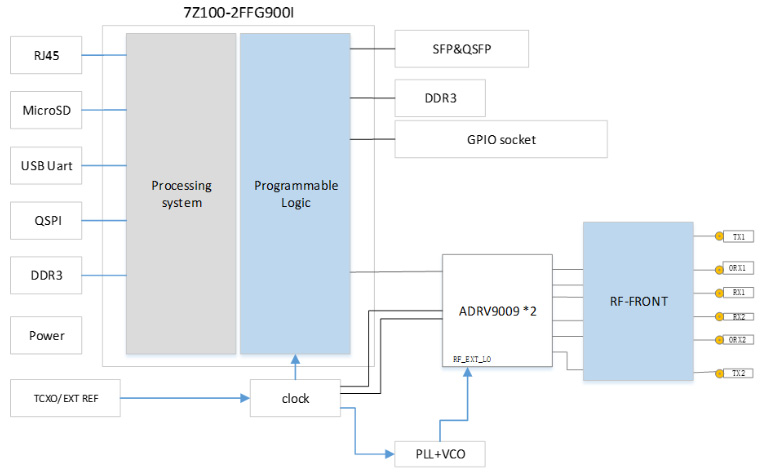
HJX-ADRV9009-X2 is highly customizable, providing wide bandwidth and tuning range for a variety of applications. It contains two broadband ADRV9009 dual transceivers, and a Xilinx Zynq7000 programmable SOC XC7Z100FFG900, which makes the entire platform have powerful data processing capabilities. At the same time, it is equipped with 1GB DDR3 dedicated to the SOC programming system part and 1GB DDR3 dedicated to the SOC programmable logic part, which provides great flexibility for developing custom applications. In addition, 256Mb flash memory is provided for data storage, and additional options are reserved for starting the system through an SD card.
HJX-ADRV9009-X2 supports board-level and inter-board phase synchronization function. High-speed data is transmitted through 40G QSFP or 10G SFP. Multiple boards can quickly build a 5G massive MIMO or phased array system, which greatly facilitates customer evaluation. The ADRV9009 transceiver includes integrated LO and phase synchronization. Using the ADI high-performance low-jitter AD9528 device, the overall system frequency and phase synchronization is maintained through a clock tree structure, making it ideal for applications that require RF phase alignment with a large number of channels.
HJX-ADRV9009-X2's RF front-end part provides hardware support for ADRV9009 RX QEC, TX QEC and LO Leakage calibration. At the same time, the RF path of the board is connected to the MM8430-2610 RF connector in series, and the input and output RF performance of the ADRV9009 chip can be directly evaluated without changing the circuit structure.
HJX-ADRV9009-X2 has a wide range of I / O functions and can use a variety of high-speed I / O, including 40G QSFP +, 10G SFP +, and Gigabit Ethernet functions. In addition, 80 pin GPIO pins are derived from different BANKs of the FPGA for communication with external modules.
HJX-ADRV9009-X2 quasi-productive circuit design ideas and programming logic allow customers to easily evaluate the design and then seamlessly integrate it into a custom carrier for further prototyping and shorten the time to market for the final product.
2. HJX-ADRV9009-X2 system technical specifications
| Technical specifications | Typical value |
Frequency tuning range | 75MHz-6000MHz |
| Maximum RX bandwidth | 200MHz |
| TX bandwidth | 450MHz |
| Maximum ORX bandwidth | 450MHz |
| ADC / DAC accuracy | 16bit/14bit |
| size | 150mm*190mm |
| Operating Voltage | 12V |
| RF interface type(MCX) | 4xTX ports 4xRX ports 4xORX ports External LO input External REF clock input SYSREF input |
3. HJX-ADRV9009-X2 interface specifications
1. Input (receive): MCX-KE (4pcs);
2. Output (transmit): MCX-KE (4pcs);
3. Feedback channel (receive): MCX-KE (4pcs);
4. External clock input interface: MCX (1pcs);
5. External local oscillator input interface: MCX (1pcs);
6. Clock chip output interface: MMCX-KE (1pcs);
7. Gigabit Ethernet port: RJ45 (1pcs);
8. SD card holder: Micro SD (1pcs);
9. 10G optical module interface: SFP (2pcs);
10. 40G optical module interface: QSFP (1pcs);
11. JTAG interface: 2X7_2.00mm (1pcs);
12. USB-UART interface: Mini-USB (1pcs);
13. Power interface: VH3.96mm 2pin (1pcs), DC-005 (1pcs);
14. Matrix connector 40Pin: 61082-04 (2pcs)
4. RF performance of RF-TX link
1. LO and image suppression indicators
Test conditions: single-tone signal mode, input frequency is set to 2080MHZ, the input power of the signal source is -12dBm, and the power output to the spectrum analyzer after the HJX-ADRV9009-X2 development board is -4.13dBm.

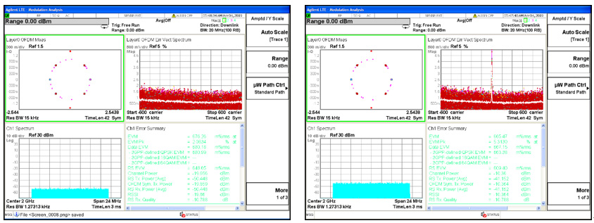
2.EVM
Test conditions: FDD-LTE signal mode, 20MHZ bandwidth, signal source input power is -19dBm, after the HJX-ADRV9009-X2 development board, the power output to the spectrum analyzer is -10.3dBm, and the EVM index is basically unchanged.

5.Application scenarios of HJX-ADRV9009-X2
? 3G / 4G / 5G TDD macro cell base stations
? TDD active antenna systems
? Massive MIMO
? Phased Array Radar
? Electronic Warfare
? Military Communications
? Portable test equipment
6、Evaluation Boards
Pricing displayed is based on 1-piece
| Model | Description | Price | RoHS |
| HJX-ADRV9009-X2 | ADRV9009 4T4R Evaluation Board | $10000.00 | Yes |
7.Contact Information
For more information or to order products, please contact Xiamen Hejiaxing Sales Office.
Mobile: +86-13600975566
WeChat:13600975566
QQ: 2355620732
Mail:zf@hjx.cn
- Case
- Repeater / Fence HPA
- MDAS
- 4G Small base station
- RFID
- Microchamber system
- Digital broadcasting
- Beidou Active System
- Shield system
- Handheld
- Tower Amplification
- Antenna board
- 5G small base station 100MW
- 5G small base station rollback
- 5G small base station DPD
- 4G+5G small base station
- V2X
- Gain Compensator
- GPS antenan
- Multi-Phase Positioning Navigation Antenna
Enterprise email:hjx@hjx.cn、zjh@hjx.cn
Mobile:13906049004(WeChat)

Xiamen Hejiaxing Electronics Co., Ltd. 閩ICP備05007801號-1


